

https://chanfifo77.tistory.com/71
[Verilog] 17. SPI Master 설계
SPI 정리 [Verilog] 16. SPI(Serial Peripheral Interface)SPI(Serial Peripheral Interface)는 Controller(Master)와 Peripheral(Slave) 간의 동기식 직렬 데이터 링크를 제공하는 통신버스입니다.Controller(Master) 장치가 CLK 신호를
chanfifo77.tistory.com

오늘은 저번 포스팅에 이어 SPI Slave와 RAM 까지 작성해보도록 하겠습니다.
SPI Slave module
Master→ → Slave
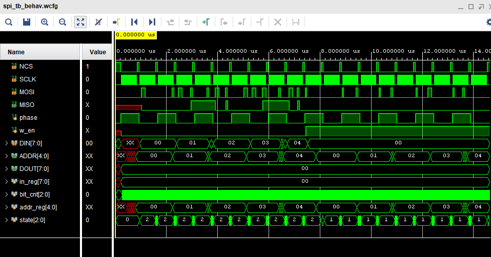
| R/W | 0 | 0 | A[4] | A[3] | A[2] | A[1] | A[0] | D7 | D6 | D5 | D4 | D3 | D2 | D1 | D0 |
Slave module에서 위의 표와 같은 순서로 8-bit nCS 8-bit 순서로 MOSI를 통해 값을 받습니다.
그 후에는 ADDR, DOUT을 통해 RAM과 데이터를 주고받고, MISO를 통해 읽을 값을 Master에게 전달하는 동작이 진행되어야 하기 때문에 Code 작성 후, Test 진행하며 수정해보도록 하겠습니다.
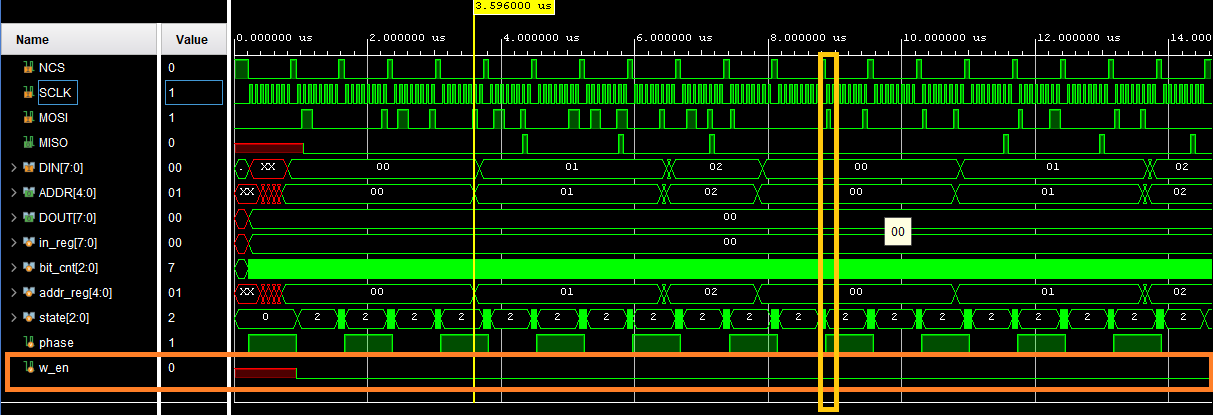
w_en 이 변하지 않는 모습입니다.
(phase = 1에서 nCS이후 1번째 bit가 1이면 Write으로 동작해야하지만 변하지 않는 모습)
- wire로 re_data추가 후 DIN과 연결하여 인스턴스
- w_en part, bit_cnt part 수정
MOSI 첫번 째 bit가 SCLK시작 전에 들어와서 끝난 후에 값이 종료되는 것 확인하였습니다. 이 펄스를 토대로
기존 w_en part의
always @ (phase) 를
always @ (posedge SCLK)로 변경하였습니다.
수정 후 phase = 1 && MOSI 1번 bit에 따라서 w_en 변화하는 모습 확인 가능합니다.
w_en = 1이 된 후에 MISO가 없어 오류가 없어 보이는 모습입니다.
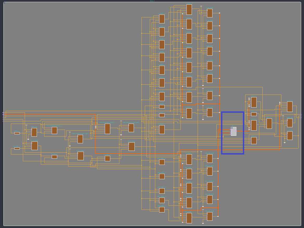
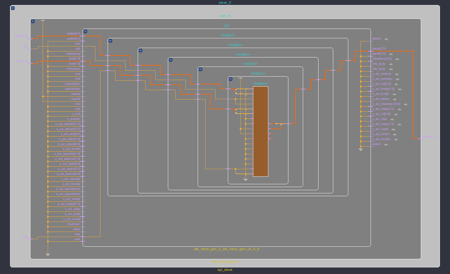
32x8 RAM
IP Catalog > RAM select
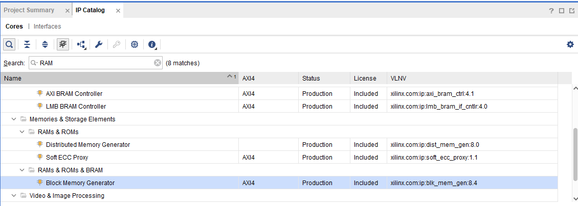
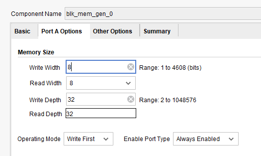
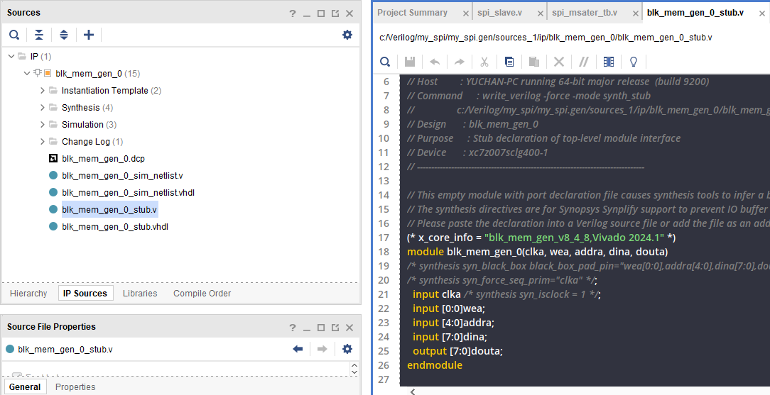
마지막으로 Slave module 에서 RAM을 Instance합니다.
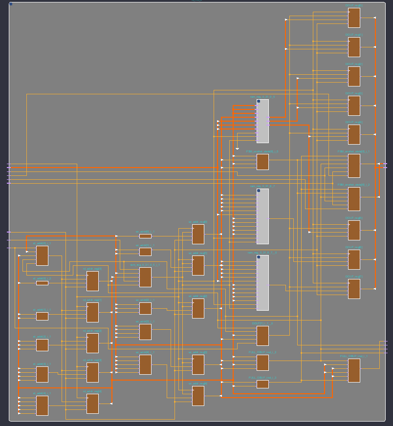
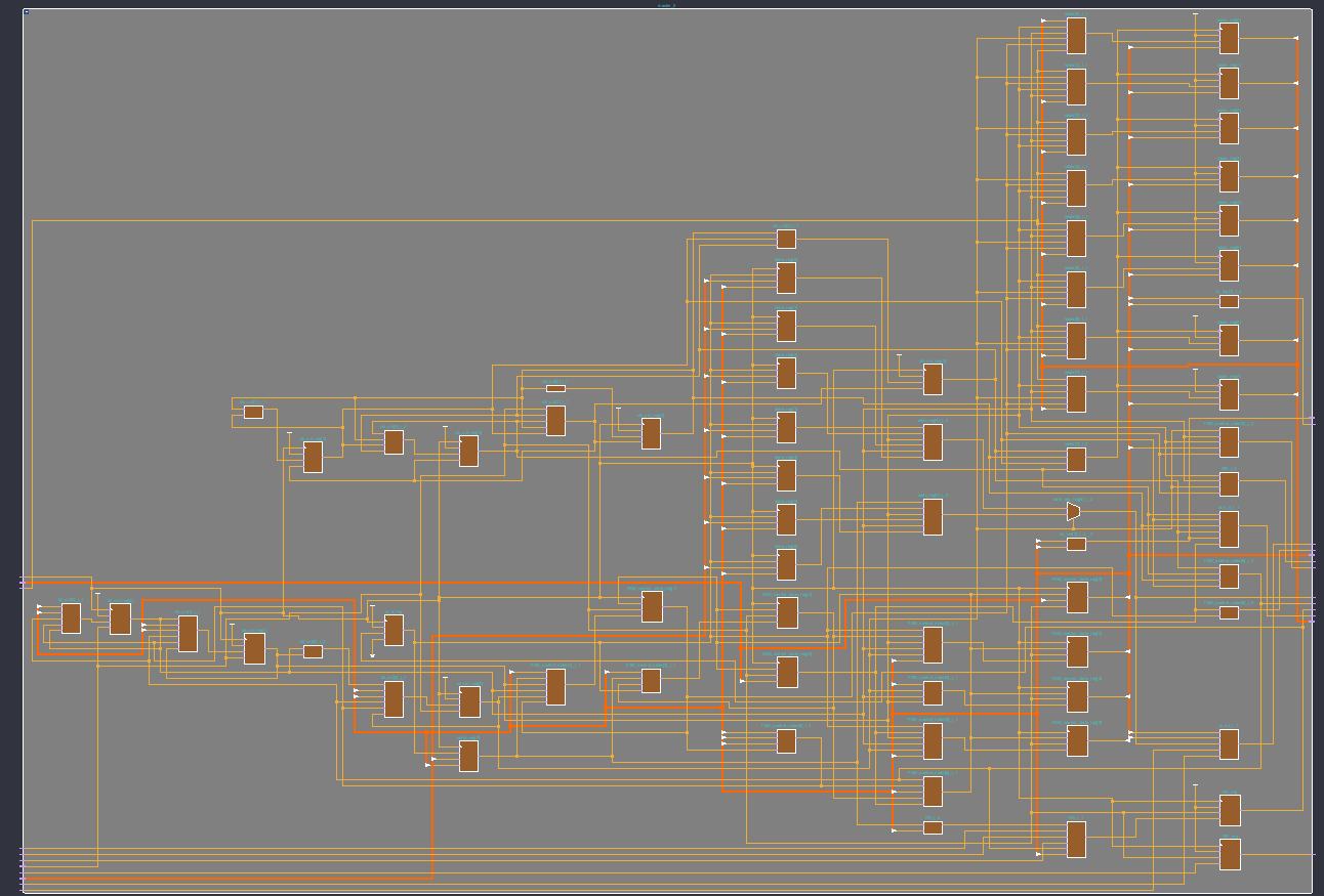
Schematic
Code
Slave Code를 마지막으로 마무리하겠습니다.
spi_slave.v 1차
invaild code
`timescale 1ns / 1ps

module spi_slave (
    input   NCS,
    input   SCLK,
    input   MOSI,
    output  reg MISO,

    input   [7:0] DIN,
    output [4:0] ADDR,
    output  [7:0] DOUT
);

reg [7:0] in_reg;
reg [2:0] bit_cnt = 3'b000;
reg [4:0] addr_reg;
reg [2:0] state;
reg phase = 0;      // 1 : Command, 0 : Data
reg  w_en;  // 1 : read enable, 0 write enable

wire [7:0] rd_data;

//Declare State Parameter
parameter [1:0] IDLE = 2'b00,
                            WRITE = 2'b01,
                            READ = 2'b10;

assign DIN = rd_data;
assign ADDR = addr_reg;     // 5-bit [4byte] data
assign DOUT = in_reg;           // 8-bit data save at register

always @ (negedge NCS) begin
    phase <= ~phase;                // Switch the Command or Data Phase
end

// w_en Part
always @ (posedge SCLK) begin      // when phase value is change
    if (phase && !NCS && (bit_cnt == 0)) begin                // former phase is R/D cmd and address
        w_en <= MOSI;
    end
end

//bit count part
always @(posedge NCS or negedge SCLK) begin
    if(NCS)begin
        state <= IDLE;
        bit_cnt <= 3'b000;
    end
    else if (!NCS) begin
        if(bit_cnt != 3'b111) begin
            bit_cnt <= bit_cnt + 1;
            end
        else if (bit_cnt == 3'b111)begin
            bit_cnt <= 3'b000;
            end
    end
end

// ADDR / DATA part
always @ (posedge SCLK or negedge NCS) begin
    // addr_reg
    // former phase
    if (phase) begin
        if (bit_cnt >= 3 && bit_cnt <= 7) begin     // if bit_cnt value is 3~7,
            addr_reg[7-bit_cnt] <= MOSI;               // Transfer MOSI's Data to addr_reg
        end
    end

    // Data Write / Read
    // latter phase
    else if (!phase) begin
        case (state)
            IDLE : begin
                in_reg <= 8'h00;                    // initialize the in_reg(connected with DOUT)
                if(w_en && !NCS)   state <= WRITE;         // change state idle to write
                else if (!w_en && !NCS) state <= READ;      // change state idle to read
            end//idle
            WRITE : begin
                if(w_en) begin
                    in_reg[(7 - bit_cnt)] <= MOSI;          // Write each Data once in SCLK
                end
                else if (!w_en) begin
                    state <= READ;                                  // change state write to read
                end
                else if (in_reg[0] == MOSI) begin       // if last data of in_reg is equal with MOSI (= when write operation is end)
                    state <= IDLE;                                  // change state write to idle
                end
            end//write
            READ : begin
                if(!w_en) begin
                    MISO <= rd_data[7-bit_cnt];                 // Read each data one in SCLK
                end
                else if (w_en) begin                       // change state read to write
                    state <= WRITE;
                end
                else if (rd_data[0] == MISO) begin         // if last data of DIN is equal with MISO (when read operatiom is end)
                    state <= IDLE;                                // change state read to idle
                end
            end//read
        endcase
    end//if(phase)
end

// Instance RAM module
blk_mem_gen_0 ram_0
(SCLK,
w_en,
addr_reg,
in_reg,
rd_data
 );

endmodule
spi_slave.v (modified)
invaild code
`timescale 1ns / 1ps

module spi_slave (
    input   NCS,
    input   SCLK,
    input   MOSI,
    output  reg MISO,

    input   [7:0] DIN,
    output [4:0] ADDR,
    output  [7:0] DOUT
);

reg [7:0] in_reg;
reg [2:0] bit_cnt = 3'b000;
reg [4:0] addr_reg;
reg [2:0] state;
reg phase = 0;      // 1 : Command, 0 : Data
reg  w_en;  // 1 : wirte enable, 0 : read enable

wire [7:0] rd_data;

//Declare State Parameter
parameter [1:0] IDLE = 2'b00,
                            WRITE = 2'b01,
                            READ = 2'b10;

assign DIN = rd_data;            // 8-bit rd_data for DIN from RAM
assign ADDR = addr_reg;     // 5-bit address
assign DOUT = in_reg;           // 8-bit data save at register

always @ (negedge NCS) begin
    phase <= ~phase;                // Switch the Command or Data Phase
end

// w_en Part
always @ (posedge SCLK) begin      // when phase value is change
    if (phase && !NCS && (bit_cnt == 0)) begin                //  first bit on positive phase
        w_en <= MOSI;                                                         // transfer to w_en
    end
end

//bit count part
always @(posedge NCS or negedge SCLK) begin     // modified (before :  always @ (NCS or negedge SCLK) but, can not use 'edge' and 'level')
    if(NCS)begin        // initialize state and bit_cnt, during nCS = 1
        bit_cnt <= 3'b000;
    end
    else if (!NCS) begin // else if nCS = 0
        if(bit_cnt != 3'b111) begin     // if bit_cnt is not full
            bit_cnt <= bit_cnt + 1;       // bit_cnt ++
            end
        else if (bit_cnt == 3'b111)begin    // if bit_cnt is full
            bit_cnt <= 3'b000;                      // initialize the bit_cnt to zero
            end
    end
end

// ADDR / DATA part
always @ (posedge SCLK or negedge NCS or posedge NCS) begin
    if(NCS) state <= IDLE;
    // addr_reg
    // former phase
    if (phase) begin
        if (bit_cnt >= 3 && bit_cnt <= 7) begin     // if bit_cnt value is 3~7,
            addr_reg[7-bit_cnt] <= MOSI;               // Transfer MOSI's Data to addr_reg
        end
    end//if(phase)

    // Data Write / Read
    // latter phase
    else if (!phase) begin
        case (state)
            IDLE : begin
                in_reg <= 8'h00;                    // initialize the in_reg(connected with DOUT)
                if(w_en && !NCS)   state <= WRITE;         // change state idle to write
                else if (!w_en && !NCS) state <= READ;      // change state idle to read
            end//idle
            WRITE : begin
                if(w_en) begin
                    in_reg[(7 - bit_cnt)] <= MOSI;          // Write each Data once in SCLK
                end
                else if (!w_en) begin
                    state <= READ;                                  // change state write to read
                end
                else if (in_reg[0] == MOSI) begin       // if last data of in_reg is equal with MOSI (= when write operation is end)
                    state <= IDLE;                                  // change state write to idle
                end
            end//write
            READ : begin
                if(!w_en) begin
                    MISO <= rd_data[7-bit_cnt];                 // Read each data one in SCLK
                end
                else if (w_en) begin                       // change state read to write
                    state <= WRITE;
                end
                else if (rd_data[0] == MISO) begin         // if last data of DIN is equal with MISO (when read operatiom is end)
                    state <= IDLE;                                // change state read to idle
                end
            end//read
        endcase
    end//if(!phase)
end

// Instance RAM module
blk_mem_gen_0 ram_0
(SCLK,
w_en,
addr_reg,
in_reg,
rd_data
 );

endmodule
https://chanfifo77.tistory.com/86
[Verilog] 20. SPI Debugging(1)
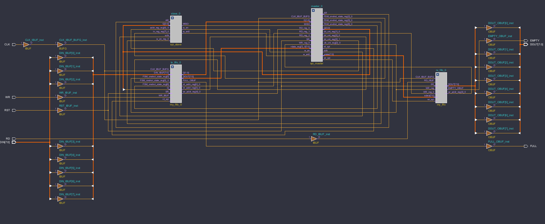
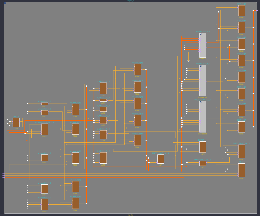
발견된 문제점1. 전제 모듈 연결 후, Read 할 때, MISO 값이 간헐적으로 이상하게 나오는 것을 확인.2. Master에서 RX FIFO로 가는 DOUT의 출력 값 이상 확인.3. Master DIN이 값을 가져오는 주기의 이상 확인.
chanfifo77.tistory.com
https://chanfifo77.tistory.com/87
[Verilog] 21. SPI Debugging (2)
https://chanfifo77.tistory.com/86 [Verilog] 20. SPI Debugging(1)발견된 문제점1. 전제 모듈 연결 후, Read 할 때, MISO 값이 간헐적으로 이상하게 나오는 것을 확인.2. Master에서 RX FIFO로 가는 DOUT의 출력 값 이상 확
chanfifo77.tistory.com
수정사항.
'Circuit Design > 🔥HDL' 카테고리의 다른 글
| [Verilog] 20. SPI Debugging(1) (0) | 2024.07.18 |
|---|---|
| [Verilog] 19. AXI Lite(AXI - Light weight) (1) | 2024.07.14 |
| [Verilog] 17. SPI Master 설계 (0) | 2024.07.02 |
| [Verilog] 16. SPI(Serial Peripheral Interface) (0) | 2024.06.27 |
| [Vitis] 1. AXI (0) | 2024.06.27 |